FPGA (Field Programmable Gate Arrays) Design
Self-paced videos, Lifetime access, Study material, Certification prep, Technical support, Course Completion Certificate
Uplatz
Summary
- Reed courses certificate of completion - Free
- Uplatz Certificate of Completion - Free
Add to basket or enquire
Overview
Uplatz provides this comprehensive course on FPGA Design & Implementation. It is a self-paced course consisting of video lectures. You will be awarded Course Completion Certificate at the end of the course.
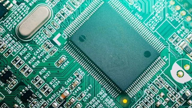
A Field-Programmable Gate Array (FPGA) is an integrated circuit designed to be configured by a customer or a designer after manufacturing – hence the term field-programmable. The FPGA configuration is generally specified using a hardware description language (HDL), similar to that used for an application-specific integrated circuit (ASIC). Circuit diagrams were previously used to specify the configuration, but this is increasingly rare due to the advent of electronic design automation tools.
FPGAs contain an array of programmable logic blocks, and a hierarchy of reconfigurable interconnects allowing blocks to be wired together. Logic blocks can be configured to perform complex combinational functions, or act as simple logic gates like AND and XOR. In most FPGAs, logic blocks also include memory elements, which may be simple flip-flops or more complete blocks of memory. Many FPGAs can be reprogrammed to implement different logic functions, allowing flexible reconfigurable computing as performed in computer software.
FPGAs have a remarkable role in embedded system development due to their capability to start system software (SW) development simultaneously with hardware (HW), enable system performance simulations at a very early phase of the development, and allow various system partitioning (SW and HW) trials and iterations before final freezing of the system architecture.
Using field programmable gate arrays (FPGAs) can significantly increase the complexity of the design process. As seen in the previous FAQ on the application considerations when selecting FPGAs, these devices can bring improved performance to complex functions and improve overall system performance. This FAQ will consider the design process for FPGAs while the next and final FAQ in this series will review system integration issues to be addressed when using FPGAs.
There are several steps in the design process when using any programmable logic, including FPGAs. These steps include design entry, design synthesis, and design verification (including functional verification and timing verification and takes places at different points during the design flow), design implementation, and device programming. The design process for FPGAs presents a variation on that basic process.
FPGA floorplanning identifies structures and functions that should be placed in proximity to each other. It can be used to reduce the amount of delay in a critical path. Floorplanning can be implemented when starting the FPGA design process before the first design iteration for design entry (place and route). It can also be used after a problem is identified during various steps of the design verification process to correct timing problems. With floorplanning, designers can identify portions of logic contributing to timing problems and correct the design entry information to reduce the routing delay.
Curriculum
Course media
Description
Course Objectives
- Learn how to model a design in Altera's ModelSim and Xilinx Isim, as well as how to programme FPGAs using the Xilinx ISE tool
- Use ModelSim to debug a VHDL design
- Use ModelSim to simulate a VHDL design
- Get to know Altera and Xilinx tools
- FPGA programming
FPGA Design & Implementation - Course Syllabus
- Introduction to FPGA (Field Programmable Gate Arrays)
- FPGA Testing
- FPGA Design Flows & Design Tools
- FPGA Design using Verilog - Introduction
- FPGA Design using Verilog - Verilog overview
- FPGA Design using Verilog - Data Types
- FPGA Design using Verilog - Procedural Assignments
- FPGA Design using Verilog - VHDL Design using Verilog
- FPGA Design using Verilog - Visual Verification of Designs
- FPGA Design using Verilog - Finite State Machines - part 1
- FPGA Design using Verilog - Finite State Machines - part 2
- FPGA Design using Verilog - Design Examples
- FPGA Design using Verilog - Test Benches
- FPGA Design using Verilog - SystemVerilog for Synthesis
- FPGA Design using Verilog - Packages & Interfaces
- Simulate and implement SOPC Design
- Reading Data from Peripherals
- UART SDRAM Python
- Script execution in Quartus and ModelSim NIOS
- Image Processing using FPGA
- Challenges in using FPAA FPGA in Mixed Signal Technology
- Protoflex
- Reconfigurable Hardware
- Wordcount using MapReduce for FPGA
- FPGA implementation of DSP Circuits
- Reversible Logic Circuits
- FPGA implementation of Divider in Finite Field
- Principles of PLI
- Spartan FPGA implementation
- Programmable Chips and Boards
- Memristive FPGA
- Mentor Graphics Tools & Guidelines
FPGAs (Field Programmable Gate Arrays) are semiconductor devices that consist of a matrix of customizable logic blocks (CLBs) linked by programmable interconnects. After production, FPGAs may be reprogrammed to meet specific application or feature needs. FPGAs differ from Application Particular Integrated Circuits (ASICs), which are custom-made for specific design needs. Although one-time programmable (OTP) FPGAs exist, the most common are SRAM-based FPGAs that can be reprogrammed as the design changes. FPGA programming has recently gained popularity due to its many advantages. It enables you to offload resource-intensive operations to hardware, resulting in improved performance. FPGAs may be programmed and reprogrammed to meet current requirements, which saves money in the long term. In this essay, I'll describe what an FPGA is, how to programme it, and how to utilise it.
It's an integrated circuit that may be configured by a user after it's been created for a particular purpose. Adaptive logic modules (ALMs) and logic elements (LEs) are coupled through programmable interconnects in modern FPGAs. These bricks combine to form a physical array of logic gates that may be configured to execute a variety of functions. This distinguishes them from other kinds of microcontrollers or Central Processing Units (CPUs), whose configuration is fixed and cannot be changed by the manufacturer.
FPGA Design is a course that teaches students how to construct and simulate their VHDL designs effectively. These designs will also be implemented on a Xilinx BASYS 3 or BASYS 2 FPGA development board so that the students may witness their ideas in action. This course teaches users how to convert their digital logic ideas into VHDL designs that can be simulated in ModelSim or ISim and then implemented on an FPGA development board from start to finish. Students will learn how to utilise Altera's tools in addition to Xilinx development boards in this course.
Who is this course for?
Everyone
Requirements
Passion & determination to achieve your goals
Career path
- FPGA Design Engineer
- FPGA Implementation Engineer
- FPGA Algorithm Engineer
- FPGA Design Consultant
- Electronics Engineer
- Embedded Engineer
- Hardware Engineer
- Firmware Engineer
- FPGA Crypto Validation Engineer
- FPGA Design Application Engineer
- FPGA/ASIC Engineer
- Electronics & Instrumentation Engineer
- Electronics Engineer VHDL FPGA
- Digital Design Engineer
Questions and answers
Currently there are no Q&As for this course. Be the first to ask a question.
Certificates
Reed courses certificate of completion
Digital certificate - Included
Will be downloadable when all lectures have been completed
Uplatz Certificate of Completion
Digital certificate - Included
Course Completion Certificate by Uplatz
Reviews
Currently there are no reviews for this course. Be the first to leave a review.

Add to basket or enquire
Course provided by
Legal information
This course is advertised on reed.co.uk by the Course Provider, whose terms and conditions apply. Purchases are made directly from the Course Provider, and as such, content and materials are supplied by the Course Provider directly. Reed is acting as agent and not reseller in relation to this course. Reed's only responsibility is to facilitate your payment for the course. It is your responsibility to review and agree to the Course Provider's terms and conditions and satisfy yourself as to the suitability of the course you intend to purchase. Reed will not have any responsibility for the content of the course and/or associated materials.
